International Exchange Award: Fabrication of GaAs Quantum Dot Chips for Scalable Quantum Optical Circuits
Posted on 9th April 2026 in News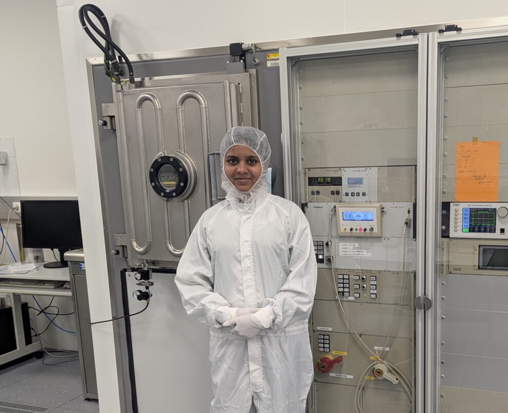 Sheena Shaji processing the GaAs quantum dot chips in the cleanroom. She is in front of the physical vapor deposition chamber where electrical contacts are deposited on the chip.
Sheena Shaji, a Post-Doctoral Research Associate at Heriot-Watt University was awarded an M4QN international exchange award to visit Prof. Armando Rastelli’s group at Johannes Kepler University. The visit took place from 8-14 March 2026.
Fabrication of GaAs Quantum Dot Chips for Scalable Quantum Optical Circuits
The aim of the visit was to jointly design a custom semiconductor quantum dot chip for scalable quantum photonic experiments and assist in the fabrication of the said chip. During the visit, Sheena worked closely with the group to design a gallium arsenide quantum dot sample incorporating multiple spatially separated, electrically gated regions. This device structure allows independent tuning of quantum dots in the different areas of a chip, enabling deterministic control of emission properties across many emitters and is designed to be compatible with our existing optical setup.
Sheena assisted the host group in the fabrication process which involved designing gate layouts, processing the quantum dot chip which included lithography, etching and metal vapour deposition, integrating electrical contacts and performing preliminary electrical and optical characterisation of the chip. The visit also provided a great learning experience in quantum dot growth and nanofabrication. They were able to successfully process a quantum dot chip with independent electrically gated regions that is compatible with the specifications of their experimental setup.
Benefits to the UK materials and quantum community
Semiconductor based self-assembled quantum dots are excellent single photon sources, offering high brightness, purity, and compatibility with semiconductor technologies. These properties make them ideal for applications in quantum communication, quantum information processing, and photonic quantum computing. Motivated by these attributes, their research seeks to move beyond demonstrations of individual emitters and address the challenge of scalability with the goal of employing quantum dots as building blocks for programmable optical circuits. To this end, they have developed a custom optical setup incorporating a spatial light modulator that enables reconfigurable and independent optical control of multiple spatially separated quantum dots within a single chip. However, utilising the full potential of the setup and creating large optical circuits requires the availability of high-quality quantum dot samples with local and independent tunability of emitters.
Prof. Armando Rastelli’s research group at Johannes Kepler University has pioneered the growth and fabrication of high-quality gallium arsenide quantum dots. The jointly designed custom quantum dot chip featuring independently gated regions to enable precise tunability over spatially separated emitters is viewed by those involved as the first step towards addressing the current bottleneck of scalable quantum photonic systems aligning with M4QN’s goals to facilitate materials research for future quantum technologies.
Visit Outcomes
The visit provided a valuable opportunity for Sheena to gain hands-on experience in the post-processing of electrically gated quantum dot chips. It also enabled them to give real time feedback on the sample design during fabrication, helping to overcome fabrication obstacles while optimizing compatibility with our existing experimental setups. Sheena was able to bring the successfully processed chip back to the laboratory at Heriot-Watt University for subsequent optical characterization and future experiments on quantum optical circuits. The visit also facilitated in-depth discussions on design improvements for future samples, informed by the insights gained during this work. They discussed more advanced processing methods like reactive ion etching for future samples to overcome some of the limitations faced during the visit.
Sheena also delivered an invited seminar to the Semiconductor Physics department at Johannes Kepler University, which lead to productive scientific discussions.
Overall, the visit has been helpful in establishing a sustained collaboration that combines Heriot-Watt University’s expertise in the optical control of quantum dots with the advances materials growth and fabrication capabilities of Prof. Armando Rastelli’s group, enabling further progress toward scalable quantum photonic devices.